- 您现在的位置:买卖IC网 > Sheet目录3871 > PIC18F1230T-I/SO (Microchip Technology)IC PIC MCU FLASH 2KX16 18SOIC
PIC18F1230/1330
DS39758D-page 142
2009 Microchip Technology Inc.
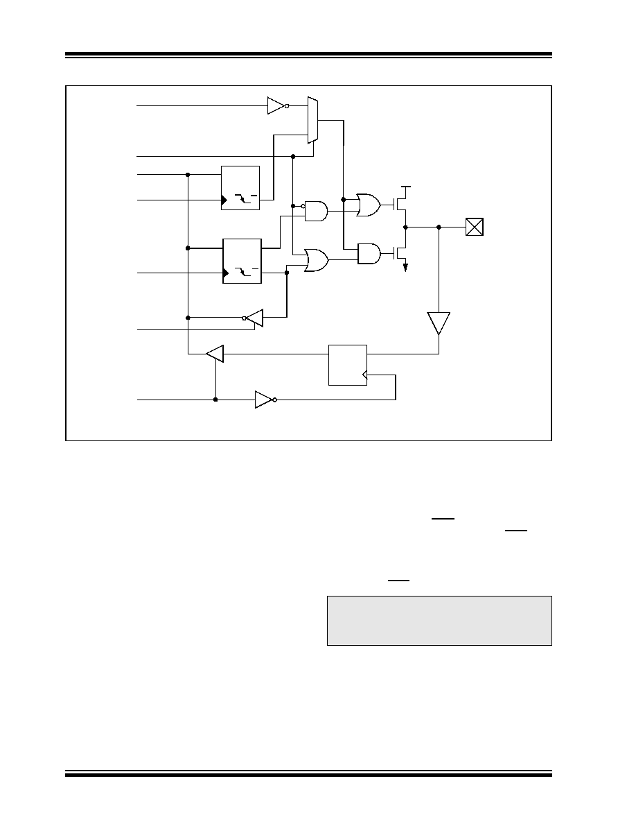
FIGURE 14-23:
PWM I/O PIN BLOCK DIAGRAM
14.11.3
PWM OUTPUT PIN RESET STATES
The PWMPIN Configuration bit determines the PWM
output pins to be PWM output pins, or digital I/O pins,
after the device comes out of Reset. If the PWMPIN
Configuration bit is unprogrammed (default), the
PWMEN2:PWMEN0 control bits will be cleared on a
device Reset. Consequently, all PWM outputs will be
tri-stated and controlled by the corresponding PORT
and TRIS registers. If the PWMPIN Configuration bit is
programmed low, the PWMEN2:PWMEN0 control bits
will be set to ‘100’ on a device Reset:
All PWM pins will be enabled for PWM output and will
have the output polarity defined by the HPOL and
LPOL Configuration bits.
14.12 PWM Fault Input
There is one Fault input associated with the PWM
module. The main purpose of the input Fault pin is to
disable the PWM output signals and drive them into an
inactive state. The action of the Fault input is performed
directly in hardware so that when a Fault occurs, it can
be managed quickly and the PWMs outputs are put into
an inactive state to save the power devices connected
to the PWMs.
The PWM Fault input is FLTA, which can come from
I/O pins, the CPU or another module. The FLTA pin is
an active-low input so it is easy to “OR” many sources
to the same input.
The FLTCONFIG register (Register 14-8) defines the
settings of the FLTA input.
14.12.1
FAULT PIN ENABLE BIT
By setting the bit FLTAEN in the FLTCONFIG register,
the corresponding Fault input is enabled. If FLTAEN bit
is cleared, then the Fault input has no effect on the
PWM module.
Data Bus
WR PORT
WR TRIS
RD PORT
Data Latch
TRIS Latch
P
VSS
I/O pin
Q
D
Q
CK
Q
D
Q
CK
Q
D
EN
N
VDD
RD TRIS
Schmitt
Trigger
TTL or
0
1
PWM Pin Enable
PWM Signal from Module
Note:
I/O pin has protection diodes to VDD and VSS. PWM polarity selection logic not shown for clarity.
Note:
The inactive state of the PWM pins is
dependent on the HPOL and LPOL Con-
figuration bit settings, which define the
active and inactive state for PWM outputs.
发布紧急采购,3分钟左右您将得到回复。
相关PDF资料
PIC18F1330T-I/ML
IC PIC MCU FLASH 4KX16 28QFN
PIC18F65J50T-I/PT
IC PIC MCU FLASH 16KX16 64TQFP
PIC18F83J11T-I/PT
IC PIC MCU FLASH 4KX16 80TQFP
PIC16LF627-04/P
IC MCU FLASH 1KX14 COMP 18DIP
PIC18F86J55T-I/PT
IC PIC MCU FLASH 48KX16 80TQFP
PIC18F43K22-I/MV
MCU PIC 8KB FLASH 40QFN
PIC16C55A-04I/P
IC MCU OTP 512X12 28DIP
PIC18LF43K22-I/MV
MCU PIC 8KB FLASH 40UQFN
相关代理商/技术参数
PIC18F1230T-I/SS
功能描述:8位微控制器 -MCU 4KB Flash 256 RAM RoHS:否 制造商:Silicon Labs 核心:8051 处理器系列:C8051F39x 数据总线宽度:8 bit 最大时钟频率:50 MHz 程序存储器大小:16 KB 数据 RAM 大小:1 KB 片上 ADC:Yes 工作电源电压:1.8 V to 3.6 V 工作温度范围:- 40 C to + 105 C 封装 / 箱体:QFN-20 安装风格:SMD/SMT
PIC18F1320-E/ML
功能描述:8位微控制器 -MCU 8KB 256 RAM 16 I/O RoHS:否 制造商:Silicon Labs 核心:8051 处理器系列:C8051F39x 数据总线宽度:8 bit 最大时钟频率:50 MHz 程序存储器大小:16 KB 数据 RAM 大小:1 KB 片上 ADC:Yes 工作电源电压:1.8 V to 3.6 V 工作温度范围:- 40 C to + 105 C 封装 / 箱体:QFN-20 安装风格:SMD/SMT
PIC18F1320-E/P
功能描述:8位微控制器 -MCU 8KB 256 RAM 16 I/O RoHS:否 制造商:Silicon Labs 核心:8051 处理器系列:C8051F39x 数据总线宽度:8 bit 最大时钟频率:50 MHz 程序存储器大小:16 KB 数据 RAM 大小:1 KB 片上 ADC:Yes 工作电源电压:1.8 V to 3.6 V 工作温度范围:- 40 C to + 105 C 封装 / 箱体:QFN-20 安装风格:SMD/SMT
PIC18F1320-E/SO
功能描述:8位微控制器 -MCU 8KB 256 RAM 16 I/O RoHS:否 制造商:Silicon Labs 核心:8051 处理器系列:C8051F39x 数据总线宽度:8 bit 最大时钟频率:50 MHz 程序存储器大小:16 KB 数据 RAM 大小:1 KB 片上 ADC:Yes 工作电源电压:1.8 V to 3.6 V 工作温度范围:- 40 C to + 105 C 封装 / 箱体:QFN-20 安装风格:SMD/SMT
PIC18F1320-E/SS
功能描述:8位微控制器 -MCU 8KB 256 RAM 16 I/O RoHS:否 制造商:Silicon Labs 核心:8051 处理器系列:C8051F39x 数据总线宽度:8 bit 最大时钟频率:50 MHz 程序存储器大小:16 KB 数据 RAM 大小:1 KB 片上 ADC:Yes 工作电源电压:1.8 V to 3.6 V 工作温度范围:- 40 C to + 105 C 封装 / 箱体:QFN-20 安装风格:SMD/SMT
PIC18F1320-H/ML
功能描述:8位微控制器 -MCU 8KB FL 256RAM 16 I/O RoHS:否 制造商:Silicon Labs 核心:8051 处理器系列:C8051F39x 数据总线宽度:8 bit 最大时钟频率:50 MHz 程序存储器大小:16 KB 数据 RAM 大小:1 KB 片上 ADC:Yes 工作电源电压:1.8 V to 3.6 V 工作温度范围:- 40 C to + 105 C 封装 / 箱体:QFN-20 安装风格:SMD/SMT
PIC18F1320-H/P
功能描述:8位微控制器 -MCU 8KB FL 256RAM 16 I/O RoHS:否 制造商:Silicon Labs 核心:8051 处理器系列:C8051F39x 数据总线宽度:8 bit 最大时钟频率:50 MHz 程序存储器大小:16 KB 数据 RAM 大小:1 KB 片上 ADC:Yes 工作电源电压:1.8 V to 3.6 V 工作温度范围:- 40 C to + 105 C 封装 / 箱体:QFN-20 安装风格:SMD/SMT
PIC18F1320-H/SO
功能描述:8位微控制器 -MCU 8KB FL 256RAM 16 I/O RoHS:否 制造商:Silicon Labs 核心:8051 处理器系列:C8051F39x 数据总线宽度:8 bit 最大时钟频率:50 MHz 程序存储器大小:16 KB 数据 RAM 大小:1 KB 片上 ADC:Yes 工作电源电压:1.8 V to 3.6 V 工作温度范围:- 40 C to + 105 C 封装 / 箱体:QFN-20 安装风格:SMD/SMT